


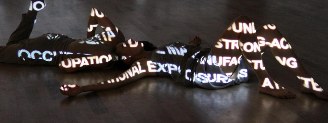


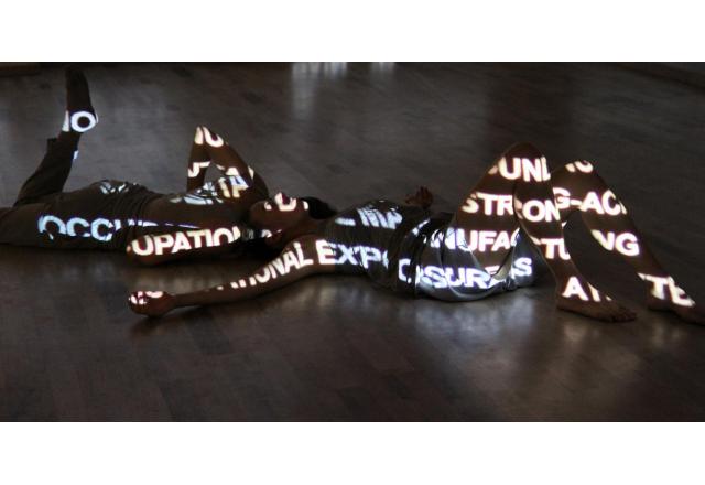
During 2015-2016 scientists and artists have found a different way and a different language to translate the scientific formulation into artistic aspects. A unique and direct meeting between the parties brings the outcome you will see here today. "Our departure as researchers outside of the campus borders and outside of the borders of ourselves as researchers, proved to be highly successful. The artists influenced the way we see our world and our researches, and this connection has opened a road to create around us a real art" according to Prof. Danny Porat.
The center for Nano-science and Nano-technology provides a basis and a wide and multidisciplinary frame that brings together researchers from various fields of research, and unifies them with researching the unique effects that occur in the Nanometric range, where the material characteristics are changing and the traditional multidisciplinary borders are blurred. The artists heard about the different physical and chemical characteristics of the Nanometric materials, and lerned from applications like: tiny sensors, drug carriers inside the body, electronic components and optical components. As a result of the conversations, the meetings and the visits in the laboratories, the artists created an artistic interpretation to the contents they have been exposed to. The Nanoart project is an outcome of the cooperation between The Hebrew University Center for Nano-science and Nano-technology, the Municipality of Jerusalem and groups from the fields of dramatic arts and plastic arts.
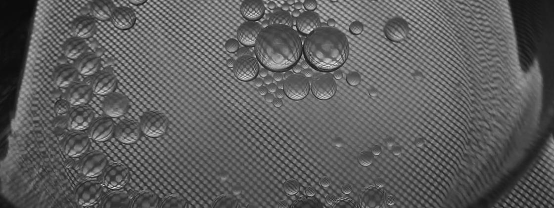
The meaning of the name "Nano" from Greek Nanos is "dwarf". It is common to think we are living in the Nano period, since this word became to be used on a daily basis, and behind it there is a scientific world that slides to the non-scientific world as well. The origin of the Nano world is in the length unit of Nanometer which equals to the length that received if we divide one meter to 1,000,000,000 equal pieces. It is clear that such a size is invisible to a naked eye, and also to the regular microscopes, and it is hard to illustrate. It is approximately the thickness of a hair which has cut to 10,000 equal pieces.
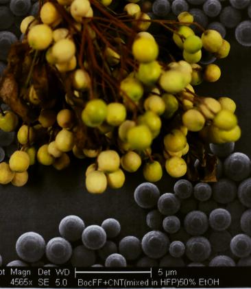
In fact, the Nano world describes objects in the size of less than 100 Nanometer, that surprisingly having different characteristics from those larger sized materials, which we can see and hold. The Nanometric objects that can have different shapes (sphere, rod etc.) are made of dozens to hundreds of atoms which are held together by Chemical forces. To the Nanometric materials there are characteristics like color, solubility, etc. that are resulting directly of their small size, and as said, they are different from the characteristics of the same materials which have a macroscopic size. For example, a Nanometric particle of gold can have red or blue color (accordingly to its size), which is different of course from the gold color we know, in the smallest objects we are able to see.
The different Physical and Chemical characteristics of Nanometric objects make them particularly attractive in many applications, such as: tiny sensors, drug carriers inside the body, electronic components and optical components. The huge research that has been made in the scientific world, and today also in the industry, tries to take advantage of the special characteristics of those materials (there are thousands of different Nanometric materials) in favor of the human beings and the mankind. Nonetheless, the people of science not once find themselves hard to explain the Nano world concept to the general public.
NanoArt team: Tirtsa Lavi, Michal Mor, Eyal Ezri, Prof. Danny Porath.